Single crystal growth in Switzerland – a flash back and outlook
By Prof. László Forró, EPFL
Materials are the linchpin of technological progress. All energy related applications like photovoltaics, fuel cells, thermoelectrics, (harvesting, storing and transmitting) heavily depend on new, more performant materials. Even the success of energy production by nuclear fusion crucially relies on finding compounds that can withstand high doses of irradiation. Information technologies are another huge field which are seeking for new materials. Their discovery and in-depth characterization happens in single crystalline form. This strategy has already been recognized since a long time ago in Switzerland, and a short summary is given below, with some thoughts about future trends.
Flash back
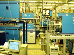
In Switzerland, there is a strong tradition for growing novel materials. Not going too far back in history, just to remind us about the heavy fermion CeAl3 discovered (1) in the laboratory of Hans-Rudi Ott, or the high temperature cuprate superconductor at IBM Rüschlikon by George Bednorz and Alex Müller (2). Traditionally, at ETHZ there was a strong competence in crystal growth, in the group of Oskar Vogt and Emanuel Kaldis. At EPFL Francis Levy started a programmed activity of which the highlights were the charged density wave systems. They were associated with the name of Helmuth Berger, a physical chemist, having a special gift and patience for growing unique single crystals. Figure 1 shows a part of his laboratory, where 30 furnaces could run simultaneously, all piloted by computer for their temperature ramps. This gives us a good illustration of a modern infrastructure for crystal growth.
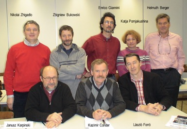
This activity developed a new dimension in the creation of the NCCR MaNEP, lead by Oystein Fischer and University of Geneva, as leading house. MaNEP has networked the whole country, and the growth of single crystals, the discovery of new materials was a strongly supported endeavor. This was the time when at Uni Geneva and at Paul Scherer Institute serious investments in crystal growth were made, (e.g. several image furnaces were installed for the travelling floating zone method), and the axis of Geneva-Lausanne-PSI-ETHZ, as strongholds in sample preparation, were established. As it happened, in MaNEP, I had the role of project coordinator of single crystal growth, and from this period at one of the regular project meetings, this “historical” photo (figure 2) was taken, with Janusz Karpinski, Nikolai Zhigadlo and Zbiegniew Bukowski from Zürich (specialists in high pressure synthesis), Kazimir Conder and Katja Pomjakushina from PSI, Enrico Giannini from Uni Geneva and Helmuth Berger from EPFL. At some point of the NCCR, Jörg Hulliger from Uni Bern for the discovery of novel superconductors, mainly using combinatorial chemistry, Reinhard Nesper and Greta Patzke with functional nano- and microstructures were associated to the network.
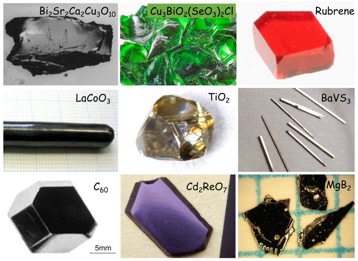
The activity of these 12 years of MaNEP gave crystals of extraordinary breadth and beauty. Many superconductors, magnetic materials, organic crystals, functional oxides, low-dimensional conductors and more were synthesized. The competition between several collective electronic interactions, the formation of novel electronic phases was preferentially addressed. A small set of crystals is shown in Fig 3. They were very precious for experimental studies and theoretical modellings. Single crystal growth has strongly contributed to the coherence of the MaNEP network, enhancing collaborations between various groups.
Present
Since the end of MaNEP in 2013, the “crystal growth landscape” has changed considerably. Some chemists, who had crucial inputs, have retired (Karpinski, Berger, Conder), and at some places the research focus has changed (shifted towards nanoscales), where e-beam lithography took the lead over crystal growth. This was the case of ETHZ, where the strong expertise in high pressure synthesis (with worldwide visibility) has disappeared. Experts like Nikolai Zhigadlo and Sergiy Katrych, temporarily employed at Uni Bern and EPFL, could not be stabilized at any of the research facilities in the country.
On the other hand, other laboratories are trying to establish their activity in the field of strongly correlated and magnetic materials. At ETHZ Frank Lichtenberg and Fabian O. von Rohr at Uni Zürich were hired bringing their knowledge in various crystal growth techniques. At Uni Bern, Karl Krämer continues the high standards established by Jörg Hulliger.
The greatest positive changes happened probably at EPFL, where the laboratory run by Helmuth Berger was taken over by Arnaud Magrez. Recognizing the importance of crystal growth at the Institute of Physics, a Coordinating Committee for the Crystal Growth Facility was created from the faculty members working in, or close to solid state physics. By a collective decision, the facility has been expanded by sample characterization equipments (x-ray, Raman, PPMS, optics) as well. Users coming from other schools and universities appreciate this service.
Beyond the domain of Arnaud Magrez, three other solid state chemists were hired, Endre Horváth, Márton Kollár and Trpimir Ivsic, working on photovoltaic materials, nanocrystals and on novel superconductors. Although these are temporary appointments, their output is already remarkable.
In terms of materials, the quest for superconductors with exotic pairing symmetry and higher Tc is and will always be a scientific driver. The latest news from Eremets group (6) and the Hemley-group (7), reporting superconductivity at 203 and 260 K in H3S and LaH10, respectively, at very elevated pressures opens the imagination of chemist, physicists to suggest compositions which at ambient conditions or at more moderate pressures could show similarly high Tc. Such a material is still to come.
There is great interest in synthesizing novel magnetic materials, which could be investigated in-depth at PSI and SLS or other user facilities abroad. The interest for a class of materials, which are hosting skyrmion structures (magnetic vortices) is expanding rapidly. One such material is Cu2OSeO3. Beyond the beauty of the magnetic motif, it seems to be very suitable for information technologies, since skyrmions are robust against defects, perturbations and they can be easily driven by electric field.
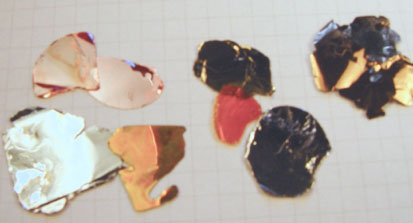
Along the same idea, looking for topologically protected structures, which could carry information, the topological insulators and Weyl semimetals were extensively studied. It seems that lately, search for similar protected states is looked for in transition metal dichalcogenides (TMDs). This class of material is very fashionable due to their proximity to graphene, to the ease with which one can exfoliate them and to study two-dimensional electronic and magnetic structures. One can even build up, like a lego, heterostructures with them, alternating magnetic and nonmagnetic layers, or having interchanging sheets with weak and strong spin orbit couplings, etc. The choice in this class of materials is tremendous. A sub-set of crystals, coming from the heritage of Helmuth Berger is shown in Figure 4.
Materials discovery traditionally is based on physical intuitions, which compound could give the desired property and functionality, followed by synthesis and characterization, and by trial-and-error, one could find the foreseen compound. Lately, a new approach, using machine learning, is becoming more and more popular and efficient. It uses databases where individual phases with their chemistry, physical properties as a function of temperature, pressure, magnetic field etc., are catalogued (the essence of the Materials Genome Initiative), and using this input one can make suggestions for compositions which could show the custom desired property. For the most promising compositions one can make detailed first principle calculations to further support the choice. It is believed that such an approach reduces the time needed for the discovery of a new material and with that the costs, as well. This strategy has been adopted also by the NCCR Marvel (with EPFL as leading house) which program is a computational design and discovery of novel materials. They are making major advances in predicting novel materials.
Outlook and utopia
One can find new materials with the help of machine learning, but they have to be synthesized in crystalline form in order to learn their intrinsic properties. If they fulfill the expectations, then their purification, processing, and increased yield production are essential steps in finding their route to targeted applications. All these steps present bottlenecks, which often hinder fundamental discoveries and set the limits for the usability of the materials.
How important the perfection of a material is, could be well illustrated by the cuprate superconductors. Lot of the relevant physics of high Tc was hidden due to the bad lousy samples, until Andreas Erb (3) in Geneva produced four nine YBCO, or at Vancouver Doug Bonn and Walter Hardy haven’t improved the quality of under-doped single crystals (4). Taking another class of materials, the topological insulators, which quality is so lousy, that they are not even insulators in the bulk, due to the defects which heavily dope the sample. This is valid for TMDs too. It is clearly seen in the case of semiconductors, like MoS2, which should have a band gap of 1.1 eV, but the electronic transport is dominated by a low-lying donor state (60 meV) coming from defects (5). So, improving the material is a primordial step towards their investigations and applications.
This task goes beyond national frontiers; it is an overall problem in material science. Developed countries put hundreds of millions in large facilities (synchrotron light sources, free electron lasers, spallation sources) but there is no commensurate increase in the ability of making new or improved quality materials. To overcome this gap, to study top quality materials, here is a suggestion, which at this moment may well sound utopic, but I think that there is a great need for it: a Material Development Center (MDC) run as user facility (like the Swiss Light Source or others).
MDC is foreseen as the first user facility to accelerate materials processing. It would provide access to a large number of processing equipments, protocols and know-how which individual laboratories in general cannot afford/maintain in house. Laboratories, which are hindered in executing their ideas, to synthesize, and process their newly discovered materials, could apply for access to the MDC facilities and to use the allotted equipment(s) and most promising protocols to accelerate material development. Review by an independent Scientific Committee will award the resources to devoted international users coming to the MDC from Europe-wide or broader.
The infrastructure should consist of i) material preparation labs; ii) crystal growth facility from nanoscale to bulk; iii) structural and chemical analysis; iv) crystal cutting/polishing/orientation lines; v) necessary inspection and characterization tools.
The MDC would elevate applied- and basic material research to a new level, creating a worldwide hub of unforetold discoveries for decades. It would create a unique research infrastructure, which would strengthen the overall impact of research. It could become the trade hall of original ideas in material synthesis.
Acknowledgment. My colleagues in Lausanne, Helmuth Berger, Francis Levy, Henrik Ronnow, Oleg Yazyev, Arnaud Magrez, Endre Horvath are gratefully acknowledged. The idea of MDC was elaborated together with Karoly Holczer (UCLA).
References:
1. K. Anders, J.E. Graebner, H.-R. Ott, Phys. Rev. Lett 35, 26 (1975)
2. J. G. Bednorz and K. A. Müller, Zeitschrift für Physik B Condensed Matter, 64, 189–193 (1986)
3. A. Erb, E. Walker, R. Flückiger, Physica C 245 (1995) 245-251
4. R. Liang, D.A. Bonn, W. N. Hardy, Physica C 336, 57-62 (2000)
5. A. Pisoni et al., Journal of Physical Chemistry C 119, 3918 (2015)
6. A. P. Drozdov et al., , Nature 525, 73-76 (2015)
7. Maddury Somayazulu et al., https://arxiv.org/pdf/1808.07695.pdf