Correlated electronic states in semiconductor moire materials

By Atac Imamoglu, ETHZ
Moire superlattices in two dimensional semiconductors constitute a new platform for strongly correlated electron physics. Even though the first publication in the field appeared in 2020, a number of breakthrough results ranging from the observation of Mott-Wigner states to quantum anomalous Hall effect have already been reported. Electrical control of charge density as well as the periodic moire potential suggests that semiconductor moire materials provide an ideal platform for investigation of quantum magnetism.
Van der Waals heterostructures of two dimensional (2D) materials constitute a new paradigm for condensed-matter physics. A subclass of particular interest for the investigation of strongly correlated electrons are semiconductor moire materials 1,2 composed of transition metal dichalcogenide (TMD) bilayers. A moire superlattice potential for electrons emerges when the two TMD layers have a lattice mismatch, or when they are stacked with a finite twist angle. Typical superlattice constants are of the order of 10 nm, generically resulting in flat electronic bands in the reduced Brilloin zone. In contrast to the extensively studied quantum materials, semiconductor moire systems provide a very high degree of tunability of the lattice parameters relevant for controlling correlations, such as the carrier density and the ratio of interaction energy to the hopping strength. Moreover, unlike cold-atom quantum simulators, physics and functionality of moire materials could be varied using readily accessible external electric and magnetic fields, creating a platform where different many body phases compete. During the first three years since the first realization of a semiconductor moire material, a wealth of correlation physics has been observed in (twisted) bilayers of TMDs 3.
Building blocks of semiconductor moire materials
There are 6 layered semiconductors whose band structure can be qualitatively understood using the massive Dirac model: these are labelled as MX2 where M stands for the metal atom (Mo or W), and X stands for the chalcogen atom (S, Se or Te). A monolayer of these materials has a honeycomb lattice structure where the metal atom (Mo or W) and the 2 chalcogen atoms (S, Se or Te) form the A and B sites. Both the conduction band (CB) minima and the valence band (VB) maxima are in the K and K’ points of the Brilloin zone (BZ), with a quasi-particle gap for free standing monolayers ranging from ~ 1.5 eV for MoTe2 to ~ 2.5 eV for WS2. Ising spin-orbit interaction ensures that the spin degeneracy is lifted for both CB and VB, leading to locked spin and valley degrees of freedom. The strength of the spin-orbit interaction ranges from 2 to 30 meV for CB and 150 to 400 meV for VB, ensuring that lowest energy optically active resonances with fixed chirality is generically valley and spin selective. CB and VB effective masses are me ~ mh ~ 0.5m0, where m0 denotes the free electron mass. Lattice constants aL of TMD monolayers with identical metal atoms differ by ≤ 1%. In contrast, pairs of monolayers, one with X=S and the other X=Se, have a lattice mismatch δ = 4%. In most experiments, the mono- or bilayer TMDs are embedded in 10 – 100 nm thick hBN layers which have a dielectric constant ε ≃ 4. By placing few-layer graphene layers on top and/or bottom of the stack, it is possible to control both the charge density as well as the out-of-plane electric field (Ez) at the location of the TMD layers. In particular, fully tunable electron/hole doping levels approaching ±1 × 1013 cm-2 is possible in a single device.
Due to the relatively large me, mh and weak dielectric screening, the optical excitation spectrum of charge-neutral TMD monolayers is dominated by excitons. The exciton binding energy hBN encapsulated monolayers is Ex ~ 200 meV, corresponding to a Bohr radius of ax ~ 1 nm. This tight confinement of excitons plays a central role in optical spectroscopy: while Ex is much higher than all other energy scales, ax remains smaller than all emerging electronic length scales such as the Fermi wavelength, the moire lattice constant aM, and the associated electronic Wannier orbital size (aW). Moreover, in the presence of itinerant electrons and holes, the tightly bound exciton can be treated as a robust and mobile polarizable quantum impurity interacting with charges. While the interaction between hole and an exciton in the same valley is weak and purely repulsive, an exciton and a hole in opposite valleys form a tightly bound molecule, termed a trion; this is an analog of the H+ ion and has a binding energy of ET ~ 25 meV. Similar arguments apply to exciton-electron interaction in MoSe2, whereas in WX2, both singlet (same valley) and triplet (opposite valley) negatively-charged trions are bound.
The exciton-electron interactions lead to a drastic modification of the optical excitation spectrum, upon injection of itinerant charges: while the exciton exhibits a blue shift that is linearly proportional to the electron density (ne), a new resonance appears that is red-shifted by ET from the original exciton resonance and gains oscillator strength with increasing ne 4,5. The quasi-particles associated with these resonances could be described as exciton-polarons: in the limit of vanishing ne, the attractive-polaron (AP) branch connects to the trion resonance whereas the repulsive polaron (RP) branch connects to the exciton resonance (X). AP excitations, which can be described as a hybrid mode of bare exciton and a collective trion excitation, is of particular interest for investigation of spin-valley physics, since the strength of K-valley AP is linearly proportional to the electron density neK′ of the K’-valley CB. Consequently, a fully spin-valley polarized electron or hole system in K’-valley CB or VB states leads to a vanishing K’-valley AP. Since the light helicity is locked to the valley degree-of-freedom, measurement of AP polarization in the circular basis directly yields the degree of magnetization.
Strong correlations in monolayer TMD: Wigner crystals
The combination of relatively heavy electron mass and reduced dielectric screening indicates that the the ratio of the characteristic Coulomb energy scale to that of kinetic energy, termed the rs parameter, exceeds 30 for ne ≤ 5 × 1011 cm-2. Consequently, for high quality TMD monolayers with low disorder, the electrons form a Wigner crystal (WC). Two recent experiments provided direct evidence for the appearance of an electronic WC even when the external magnetic field B = 0. In the absence of electrons, or when the electrons form a Fermi liquid, translational invariance ensures the presence of a single 1s TE-polarized exciton, or RP, band with parabolic dispersion. Upon formation of a WC however, excitons experience a periodic potential stemming from interactions with the ordered electrons: Bragg-umklapp scattering leads to the formation of a new exciton band in the reduced-BZ with an energy splitting given approximately by the kinetic energy of the zone-edge exciton 6, which is in turn linearly proportional to the electron density. Experiments in monolayer MoSe2 have clearly demonstrated the existence of this umklapp resonance 7. This observation, together with the concurrent experiments carried out in bilayer MoSe2, clearly demonstrate the potential of TMD materials for exploration of strong electronic correlations using optical spectroscopy.
Semiconductor moire materials
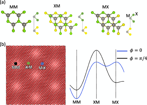
When two TMD monolayers are stacked on top each other, the C3 symmetry is retained only in three stacking configurations: for 0-degree, or equivalently AA stacking these are denoted as M-X, M-M and X-M: here, M-X denotes a registry where a top layer metal atom is placed on top of the two chalcogen atoms in the bottom layer (Fig. 1). For 180-degree, or equivalently AB stacking, the corresponding C3 symmetric registries are M-M, X-X and M-X/X-M. If the two monolayers are stacked with a finite twist angle θt, or if they have a different aL, then each one of these stacking configurations form a triangular lattice with  . A combination of lattice reconstruction, inter-layer tunneling and electrostatic potentials from inter-layer dipoles lead to the formation of a moire superlattice potential that generically has its minima and maxima at these high-symmetry points. In the long moire lattice limit (aM ≫ aL), the low energy electron or hole dynamics is captured by a continuum approximation where the Hamiltonian is given by 8

where

Here

are reciprocal moire vectors, and r = 0 for the M-M point within the moire unit cell. For AA stacked bilayers and φ ≃ 0, the moire potential leads to a single band Hubbard model with a potential depth of ≃ 12V 0 located at the M-M site (Fig. 1). DFT calculations yield potential wells with depths 50 – 100 meV. Since the kinetic energy Ekin scales with 1∕aM2, for most moire structures Ekin ≤ 10 meV. Consequently, the lowest energy TMD bilayer moire bands are generically flat bands. The on-site Coulomb interaction, which scales inversely with the reciprocal Wannier orbital size ( ), is of comparable order of magnitude with the moire potential depth. Remarkably, the strength of the nearest-neighbor Coulomb interactions in moire superlattices generically exceeds Ekin, heralding the importance of long-range correlations.

Two classes of TMD bilayer structures have been studied. In most heterobilayer systems, the band alignment is type-II, indicating that the lowest energy moire bands are exclusively located in one of the two layers, with the other layer providing the superlattice potential. The role of the layers is reversed for electrons and holes: for example, in WSe2/WS2 or WSe2/MoSe2 heterobilayers the hole (electron) lowest energy moire band is located in the WSe2 (WS2 or MoSe2) layer. Both electronic and hole moire bands in these structures are topologically trivial and realize an extended Fermi-Hubbard model.
The tell-tale of moire physics in heterobilayers is the appearance of additional intra-layer excitonic resonances when the layers are free of itinerant charges. Since the electron and hole moire potentials are not identical, there is a residual periodic potential experienced by the neutral excitons. Unlike the umklapp resonances that appear due to WC formation in monolayer TMDs, this external exciton moire potential is strong compared to the characteristic kinetic energy scale, leading to optical resonances that are split by as much as 50 meV and with sizeable oscillator strengths. Photoluminescence (PL) in these structures however, is dominated by inter-layer excitons that have a smaller resonance energy and long lifetimes due to spatial separation of electron and hole wavefunctions.
Injection of itinerant electrons and holes lead to optical excitation spectra that can differ substantially from that of monolayers. This could be understood as arising from the differences in the ability of moire electrons or holes to dynamically screen the exciton. For integer or commensurate fractional filling of moire lattice sites, the electrons (holes) form incompressible Mott-Wigner states 9,10. The large excitation gap of these correlated states in turn inhibit the ability of electrons to screen the exciton, leading to the appearance of cusps in the AP or RP spectra. Arguably, the presence of Mott-Wigner states is most spectacularly observed by monitoring the Rydberg exciton spectrum of a nearby ”sensing layer.”
MoSe2/WS2 and MoTe2/WSe2 heterobilayers differ from the others in that they exhibit a type-I band alignement when Ez = 0. Moreover, the conduction (valence) band alignement of MoSe2/WS2 (MoTe2/WSe2) can be modified by applying a large Ez. While no indication for band hybridization is observed for MoSe2/WS2, it has been shown that in AB-stacked MoTe2/WSe2 the MoTe2 and WSe2 VBs hybridize under large Ez to yield Chern bands. A direct evidence for the existence of Chern bands is evidenced by the observation of quantum anomalous Hall effect in transport measurements 11.
The second class of semiconductor moire materials consist of twisted homobilayers 12. Correlated Mott states have been observed both in AA and AB stacked twisted WSe2 homobilayers. Optical spectroscopy is partially hindered in these structures since either the CB minima (W based materials) or the VB maxima (Mo based materials) are not located in K and K’ valleys in homobilayers, ensuring that inter-valley dark excitons are the lowest energy optical excitations. A homobilayer can be rendered direct band-gap by introducing monolayer hBN in between two identical bilayers: correlated Mott states and layer ferromagnetism was observed in AA stacked twisted MoSe2/hBn/MoSe2 structures 13,14.
Outlook
The emergence of robust Mott-Wigner states forms the starting point for exploration of quantum magnetism in TMD moire structures. While preliminary high temperature experiments indicate Curie-Weiss temperatures consistent with both ferromagnetic and anti-ferromagnetic correlations for different moire lattice filling factors, a thorough investigation of magnetization at millikelvin temperatures is missing. These experiments are expected to shed light on the interplay between exchange interaction favoring 120-degree Neel order of correlated electrons in Mott-states, and kinetic energy favoring ferromagnetic order for filling factors exceeding unity.
1 Rafi Bistritzer and Allan H. MacDonald, “Moiré bands in twisted double-layer graphene,” Proceedings of the National Academy of Sciences 108, 12233–12237 (2011).
2 Eva Y. Andrei, Dmitri K. Efetov, Pablo Jarillo-Herrero, Allan H. MacDonald, Kin Fai Mak, T. Senthil, Emanuel Tutuc, Ali Yazdani, and Andrea F. Young, “The marvels of moirématerials,” Nature Reviews Materials 6, 201–206 (2021).
3 Jie Shan Kin Fai Mak, “Semiconductor moire materials,” Nature Nanotechnology (2022).
4 Meinrad Sidler, Patrick Back, Ovidiu Cotlet, Ajit Srivastava, Thomas Fink, Martin Kroner, Eugene Demler, and Atac Imamoglu, “Fermi polaron-polaritons in charge-tunable atomically thin semiconductors,” Nature Physics 13, 255–261 (2016).
5 Dmitry K. Efimkin and Allan H. MacDonald, “Many-body theory of trion absorption features in two-dimensional semiconductors,” Physical Review B 95, 035417 (2017).
6 Yuya Shimazaki, Clemens Kuhlenkamp, Ido Schwartz, Tomasz Smoleński, Kenji Watanabe, Takashi Taniguchi, Martin Kroner, Richard Schmidt, Michael Knap, and Ataç Imamoğlu, “Optical signatures of periodic charge distribution in a mott-like correlated insulator state,” Phys. Rev. X 11, 021027 (2021).
7 Tomasz Smoleski, Pavel E. Dolgirev, Clemens Kuhlenkamp, Alexander Popert, Yuya Shimazaki, Patrick Back, Xiaobo Lu, Martin Kroner, Kenji Watanabe, Takashi Taniguchi, and et al., “Signatures of wigner crystal of electrons in a monolayer semiconductor,” Nature 595, 5357 (2021).
8 Yang Zhang, Noah F. Q. Yuan, and Liang Fu, “Moiré quantum chemistry: Charge transfer in transition metal dichalcogenide superlattices,” Phys. Rev. B 102, 201115 (2020).
9 Emma C. Regan, Danqing Wang, Chenhao Jin, M. Iqbal Bakti Utama, Beini Gao, Xin Wei, Sihan Zhao, Wenyu Zhao, Zuocheng Zhang, Kentaro Yumigeta, Mark Blei, Johan D. Carlstrm, Kenji Watanabe, Takashi Taniguchi, Sefaattin Tongay, Michael Crommie, Alex Zettl, and Feng Wang, “Mott and generalized wigner crystal states in WSe2/WS2 moiré superlattices,” Nature 579, 359–363 (2020).
10 Yanhao Tang, Lizhong Li, Tingxin Li, Yang Xu, Song Liu, Katayun Barmak, Kenji Watanabe, Takashi Taniguchi, Allan H. MacDonald, Jie Shan, and Kin Fai Mak, “Simulation of hubbard model physics in WSe2/WS2 moiré superlattices,” Nature 579, 353–358 (2020).
11 Bowen Shen Yang Zhang Lizhong Li Zui Tao Trithep Devakul Keni Watanabe Takashi Taniguchi Liang Fu Jie Shan Kin Fai Mak Tingxin Li, Shengwei Jiang, “Quantum anomalous hall effect from intertwined moire bands,” Nature 600, 641 – 646 (2021).
12 Lei Wang, En-Min Shih, Augusto Ghiotto, Lede Xian, Daniel A. Rhodes, Cheng Tan, Martin Claassen, Dante M. Kennes, Yusong Bai, Bumho Kim, Kenji Watanabe, Takashi Taniguchi, Xiaoyang Zhu, James Hone, Angel Rubio, Abhay N. Pasupathy, and Cory R. Dean, “Correlated electronic phases in twisted bilayer transition metal dichalcogenides,” Nature Materials 19, 861–866 (2020).
13 Yuya Shimazaki, Ido Schwartz, Kenji Watanabe, Takashi Taniguchi, Martin Kroner, and Ataç Imamoğlu, “Strongly correlated electrons and hybrid excitons in a moiré heterostructure,” Nature 580, 472–477 (2020).
14 Ido Schwartz, Yuya Shimazaki, Clemens Kuhlenkamp, Kenji Watanabe, Takashi Taniguchi, Martin Kroner, and Ata Imamolu, “Electrically tunable feshbach resonances in twisted bilayer semiconductors,” Science 374, 336–340 (2021), https://www.science.org/doi/pdf/10.1126/science.abj3831.


